
As the US stock market approached the last trading day before the Christmas holiday, Intel, the American chip company that has just experienced a tumultuous year, encountered another modestly negative development.
On Wednesday, prior to the market opening, an article citing numerous 'informed sources' and describing $Intel (INTC.US)$ CEO Lip-Bu Tan’s interactions with the White House concluded with the following statement:
Two informed sources stated that NVIDIA recently tested whether to use Intel’s 18A process technology to manufacture its chips, but subsequently halted the initiative. NVIDIA did not respond to requests for comment.
 Additionally, in the description of the U.S. government's investment in Intel, it was noted that “foreign chip manufacturers operating in the U.S.” expressed concerns that government officials might favor directing customers toward Intel rather than cooperating with them. In response, an anonymous official from the U.S. Department of Commerce stated that the government's equity stake provides Intel with an opportunity for success but does not grant it any unfair advantages, and Intel is not “too big to fail.”
Under the impact of these two developments, Intel's shares fell more than 5% in pre-market trading. As of the time of writing, the decline had narrowed to 2% after the market opened. The company’s year-to-date gains remain at 77%.
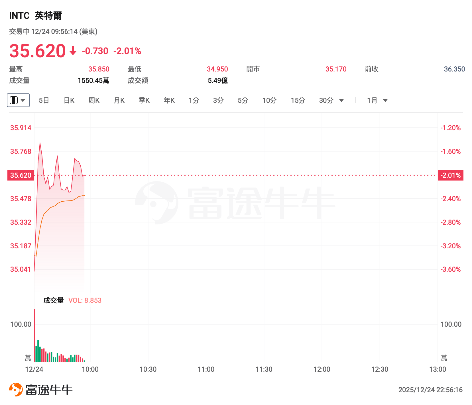
(Source: TradingView)
As context, ten years ago, after suffering a severe setback in the battle for the “10nm” process, Intel fell significantly behind Taiwan Semiconductor and Samsung in the chip manufacturing sector. After a leadership change in 2021, then-CEO Patrick Gelsinger launched a catch-up strategy aiming to close the gap with the two rivals within five years. In March this year, industry veteran Lip-Bu Tan assumed the role of Intel’s CEO and continued to focus on advancing foundry technology.
With 2026 approaching, Intel will have its first opportunity to compete head-to-head with Taiwan Semiconductor and Samsung in the 2nm process node.
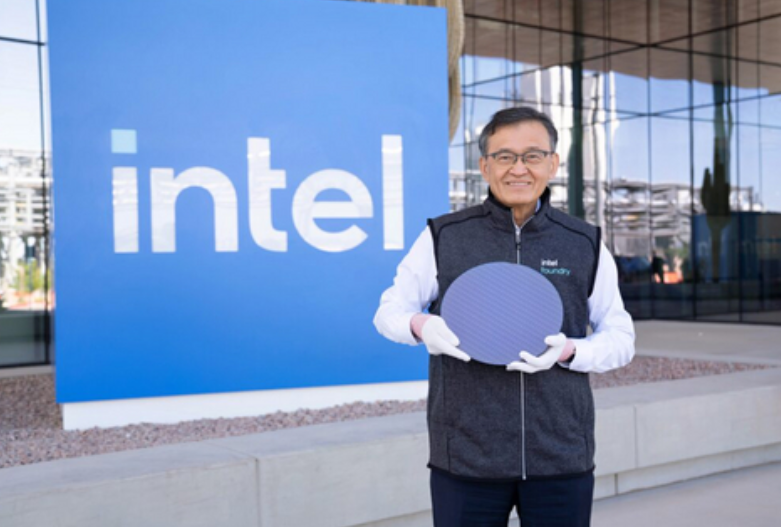
In early October this year, Intel released a photo of Lip-Bu Tan holding a wafer of the next-generation Core processor, reportedly the first chip of the next-generation Panther Lake processor manufactured using Intel’s 18A process (18 angstroms, or 1.8 nanometers). The company disclosed that mass production of Panther Lake would commence at the Fab 52 facility in Arizona later this year.
According to Intel, compared to Lunar Lake—referred to as the “pinnacle of Intel CPU energy efficiency”—Panther Lake delivers a 50% performance improvement at the same power consumption level. Additionally, at equivalent performance levels, it reduces power consumption by 30% compared to the previous-generation Arrow Lake-H processor.
As the chip bearing "Intel's hope for a turnaround," both the tech and investment communities are focused on two major mysteries surrounding Panther Lake: first, the actual performance of Intel's 18A chips; second, there have been repeated reports of negative news regarding the yield and production capacity of the 18A process.
C. C. Wei, Chairman and CEO of Taiwan Semiconductor, also stated last year that TSMC’s 3nm process is superior to Intel’s 18A in terms of performance, energy efficiency, and reliability.
In the face of such provocation, the burden on Panther Lake has become even heavier.
According to the schedule, Intel will launch the Core Ultra 300 series (Panther Lake) processors at the CES exhibition in two weeks. Some early benchmark scores have also begun to appear on the CPU benchmarking platform Geekbench. Last week, the market was astonished by a new CPU labeled “Ultra 7 365,” which scored 2451 in single-core and 9714 in multi-core tests on Geekbench 6.3. By comparison, the previous generation chip, Ultra 7 268V manufactured using TSMC’s 3nm process, scored 2639 in single-core and 10318 in multi-core.
Both chips adopt an architecture with 4 P-cores and 4 LP-E cores. However, the maximum turbo frequency of Ultra 7 268V can reach 5.0GHz, while Ultra 7 365 can only achieve 4.7GHz.
Against the backdrop of these issues, whether NVIDIA adopts 18A seems less significant. Intel has repeatedly stated that 18A is primarily intended to validate the results of its latest cutting-edge processes, with external customers expected to adopt the technology en masse only with the next-generation 14A process. During the CEO livestream event following NVIDIA’s investment in Intel, Lip-Bu Tan also noted that the agreement signed between the two companies focuses on collaboration within the x86 domain and does not cover any foundry-related matters.
Previously, renowned tech analyst Ming-Chi Kuo also revealed that Apple, Meta, and Google could all potentially become customers of Intel's 18A process technology, but mass production is not expected until at least 2027.
Editor/Doris