
①From March 16 to 19, NVIDIA GTC 2026 will be held as scheduled in San Jose, California, USA; ②Jensen Huang revealed that this GTC will unveil "a chip that will astonish the world"; ③Nomura Orient International Securities noted that investors will look forward to NVIDIA disclosing more roadmap details of its CPO technology.
Next week (March 16 to 19), NVIDIA's annual developer conference (GTC 2026), often referred to as the 'AI Spring Festival Gala,' will take place as scheduled in San Jose, California, USA.
According to the official website, Jensen Huang will deliver a keynote speech at 11:00 AM local time on March 16. Recently, Huang hinted that this GTC will unveil "a chip that will astonish the world," with significant leaps in both performance and design.
 Related articles:
Based on comprehensive information from various sources,$NVIDIA (NVDA.US)$NVIDIA is expected to unveil a new chip architecture along with multi-dimensional technological innovations at GTC 2026. According to a research report by Guolian Minsheng Securities, following the confirmation of mass production for the Vera Rubin platform at CES 2026, GTC 2026 is anticipated to feature the official debut of its enhanced version, Rubin Ultra, and may also provide an early glimpse into the preliminary technical roadmap for the next-generation Feynman architecture.
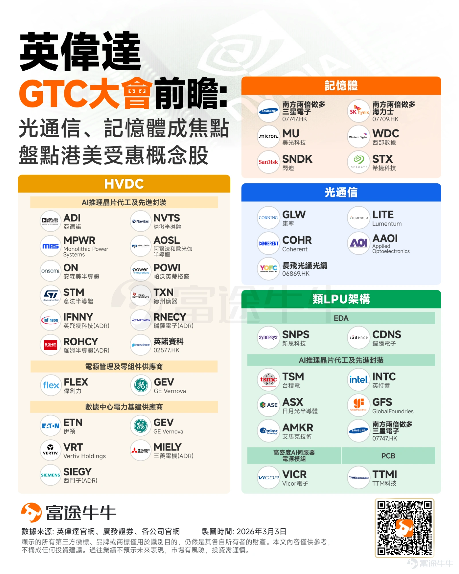
The institution stated that as power consumption continues to increase for chip architectures such as Rubin and Feynman, upgrades to power architecture and the adoption of liquid cooling technology have become critical bottlenecks for ensuring stable system operation. In terms of power systems, Rubin Ultra is expected to adopt an 800V HVDC solution, and the GTC conference may showcase modular/vertical power delivery technologies.
In the field of thermal management, the Rubin platform architecture has established full liquid cooling as a standard feature. Cold plate materials are expected to gradually upgrade from copper to copper alloys and even diamond, with liquid metal receiving authoritative certification from NVIDIA and being implemented in applications, achieving simultaneous breakthroughs in overall cooling solutions and materials.
In addition to the new architecture and supporting technologies, NVIDIA plans to launch a new inference chip integrating Groq LPU technology to address the high-performance, low-cost demands of AI inference and industry competition. Reports indicate that Groq, founded by former core members of Google's TPU team, granted its technology license to NVIDIA in 2025 and transferred 90% of its workforce. According to ChosunBiz, Groq recently decided to increase LPU production, with wafer output expected to rise from approximately 9,000 to around 15,000.
According to Guohai Securities, Groq LPU is specifically designed for inference acceleration, utilizing SRAM storage units closer to the computing core to store model parameters. With 230MB of on-chip SRAM providing up to 80TB/s of memory bandwidth, it far surpasses GPU architectures in data processing speed. Additionally, Groq employs a distributed inference strategy: creating a cluster of interconnected thousand-card units, where each card stores and computes only a small portion of the model before aggregating outputs, making it better suited for low-latency inference scenarios.
Beyond the aforementioned content, Nomura Orient International Securities noted that investors will anticipate NVIDIA disclosing more roadmap details of its co-packaged optics (CPO) technology. They will also focus on information regarding its co-packaged optical switches for scale-out networks, including Quantum-X for infinite bandwidth and Spectrum-X for Ethernet, as well as announcements of potential supply chain partners.
The institution forecasts that market penetration for scale-out co-packaged optical switches will remain low during 2026-2027 (with shipments reaching approximately 53,000 units and an 8% penetration rate by 2027). However, NVIDIA’s likely introduction of a bundling sales strategy could drive product sales beyond expectations.
Notably, the Optical Fiber Communication Conference and Exhibition (OFC) will be held concurrently with the GTC conference from March 15 to 19. The event is expected to define several key trends in the optical communication industry, including mass production and evolution of traditional optical modules at 1.6T and 3.2T, co-packaged optics (CPO) and optical I/O, optical circuit switching (OCS), as well as next-generation optical fibers and space communications.
Editor/Rice