
SemiAnalysis has conducted its first in-depth analysis of NVIDIA's Blackwell architecture: under AI workloads, tensor cores and memory bandwidth approach their theoretical peak performance overall. However, the performance heavily relies on instruction shapes and software optimization. The 2SM MMA achieves near-perfect scalability, but SMEM bandwidth and cross-Die latency of approximately 300 cycles have emerged as critical bottlenecks. The research highlights that the realization of Blackwell’s performance is not constrained by hardware limits but rather hinges on scheduling and optimization capabilities.
$NVIDIA (NVDA.US)$ The Blackwell GPU represents one of the most significant microarchitectural transformations in GPUs in recent years, yet a detailed official white paper remains unavailable.
SemiAnalysis, a renowned semiconductor research institute, conducted systematic micro-benchmarking on the Blackwell architecture over several months and, for the first time, disclosed data on the hardware performance ceiling of the architecture under AI workloads.
 The test results show that Blackwell approaches the theoretical peak in key dimensions such as Tensor Core throughput, memory subsystem bandwidth, and the new 2SM MMA instructions. However, its performance is highly dependent on instruction shape configurations, with noticeable bandwidth bottlenecks in certain scenarios. This finding has direct implications for AI infrastructure investors and chip buyers—the extent to which the architecture’s potential can be unleashed depends on fine-tuning at the software level.
SemiAnalysis has open-sourced the relevant benchmarking codebase, with the B200 nodes used for testing provided by NEBIUS and Verda. The research team also announced plans to expand their benchmarking to include TPU Pallas kernels, Trainium NKI kernels, and AMD CDNA4 assembly.
Core architectural changes: Introduction of TMEM and 2SM MMA
From Hopper to Blackwell, NVIDIA implemented several critical adjustments to the PTX abstraction layer for MMA-related instructions.
The most notable change is the introduction of Tensor Memory (TMEM) for storing MMA accumulators. In previous architectures, threads implicitly held MMA computation results; Blackwell instead adopts an explicit software management of TMEM within the MMA scope, altering the ownership relationship between threads and computation results.
At the same time, tcgen05 operations are now issued by a single thread representing the entire CTA (Cooperative Thread Array), rather than by warp or warpgroup units as in the Hopper architecture. This change is directly reflected in CuTe MMA atoms: Blackwell uses ThrID = Layout<_1>, whereas Hopper uses ThrID = Layout<_128>.
Blackwell also introduces TPC-scoped TMA and MMA, enabling two cooperative CTAs across SMs to execute tcgen05.mma while sharing operands. This reduces shared memory bandwidth requirements per CTA while providing higher-intensity MMA instructions. Additionally, the architecture natively supports sub-byte data types with scaling and introduces Cluster Launch Control (CLC) as hardware support for dynamic workload scheduling in persistent CTA kernels.
Chip Physical Layout: Dual-Die Architecture and 300-Cycle Cross-Die Latency
Through reverse engineering, SemiAnalysis unveiled the physical topology of the B200 chip.
The research team utilized the PTX %%smid instruction to infer the mapping relationship from SMs to GPCs (Graphics Processing Clusters) by launching clusters of varying sizes. The results revealed that some TPCs in the B200 are exclusively assigned to specific GPCs and are never co-scheduled with other TPCs.
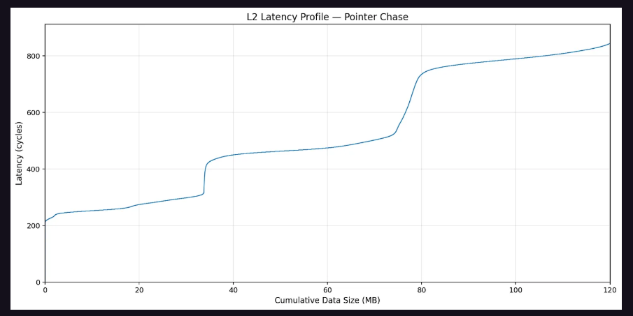
By having each SM traverse a pointer-chasing array that fills the L2 cache and measuring access latency between SMs, the research team constructed an inter-SM distance matrix. This matrix clearly delineated two groups of SMs, with an average L2 access latency difference exceeding 300 clock cycles, corresponding to the cross-Die access penalty between the two Dies.
Based on this, the research team inferred the Die-level TPC distribution of the B200 as follows:
Die A: Each GPC contains 10, 10, 10, and 9 TPCs respectively.
Die B: Each GPC contains 9, 9, 9, and 5+3 TPCs respectively.
This difference in physical layout implies that even if two GPUs have identical logical configurations, their physical SM distributions may differ, constituting a potential source of performance non-determinism.
Memory Subsystem: Performance Boundaries of LDGSTS and TMA
The memory subsystem testing focused on two types of asynchronous copy instructions: LDGSTS (asynchronous copy) and TMA (Tensor Memory Accelerator).
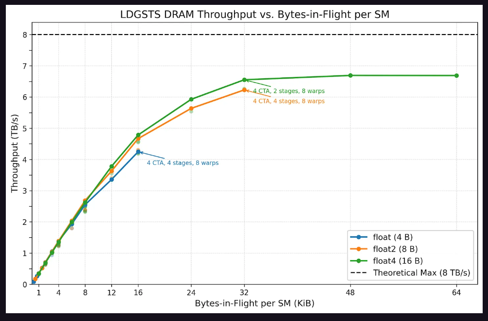
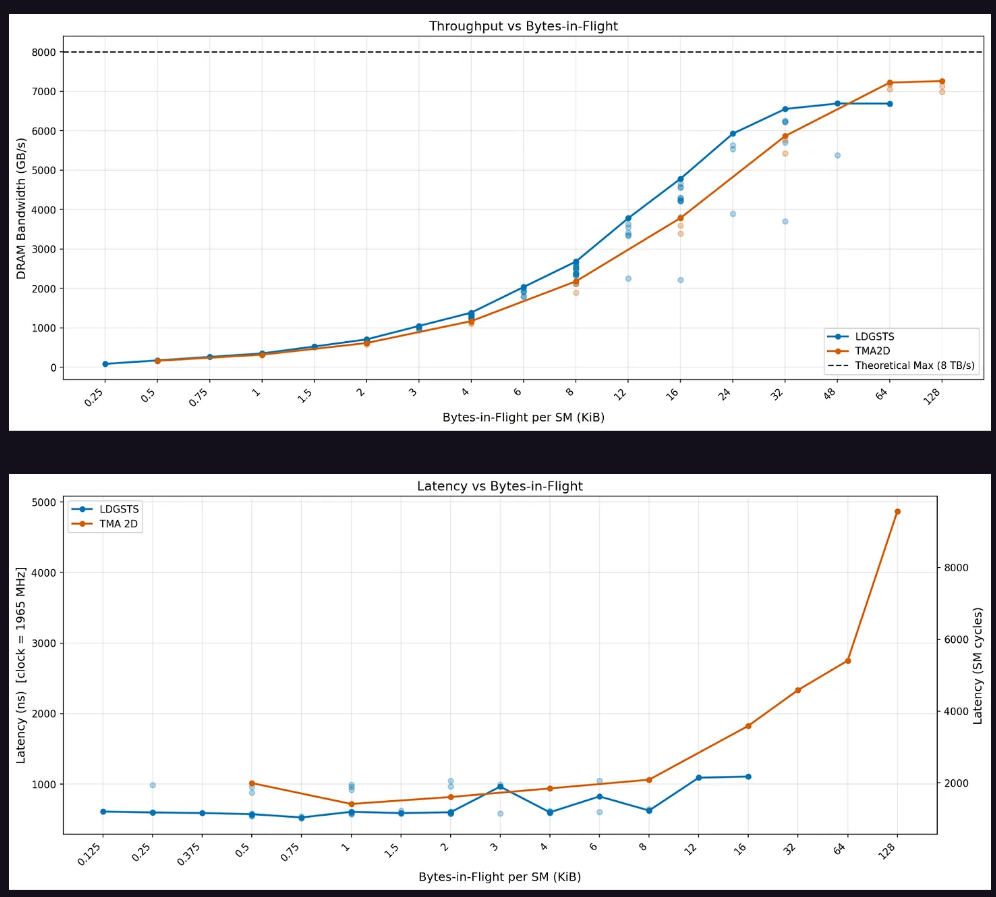
For LDGSTS, the testing covered typical configurations of the FlashInfer multi-head attention (MHA) kernel. The results showed that LDGSTS memory throughput saturated at 32 KiB in-flight bytes, with a peak of approximately 6.6 TB/s. Sixteen-byte loads performed slightly better than eight-byte loads at the same in-flight byte count while consuming fewer execution resources. Latency testing indicated a baseline LDGSTS latency of around 600 nanoseconds, which nearly doubled when the in-flight bytes exceeded 8 KiB, primarily due to thread stalls caused by MIO (Memory Input/Output) throttling.
In terms of TMA, the peak throughput is reached significantly later than LDGSTS. When the in-flight data is below 32 bytes, the asynchronous copy throughput slightly outperforms TMA; after exceeding this threshold, TMA catches up and can sustainably scale up to 128 KiB. Regarding latency, the asynchronous copy exhibits slightly lower latency when in-flight data is below 12 KiB, but TMA latency rises sharply beyond that point.
TMA multicast testing shows that explicit TMA multicast can perfectly eliminate L2 traffic, achieving the ideal "1/cluster size" L2 byte ratio. Implicit multicast (where each CTA independently issues TMA loads to the same data) performs comparably in terms of effective memory throughput, but the reduction in L2 cache traffic begins to decline after exceeding 64 bytes of in-flight data.
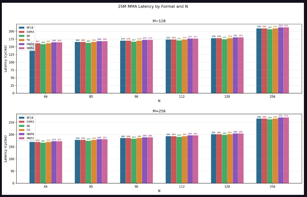
Tensor Core Performance: Significant shape dependency, with 2SM MMA achieving perfect weak scaling.
The Tensor Core test is a core component of this study, and the results reveal a high sensitivity of Blackwell MMA performance to instruction shape.
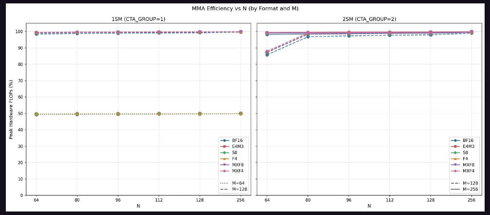
In terms of throughput, for 1SM MMA, the configuration with M=64 achieves only up to 50% of the theoretical peak, while M=128 approaches 100%. This confirms that M=64 utilizes only half of the data path. For 2SM MMA, M=128 achieves 90% of the peak throughput at N=64, with other N dimensions approaching nearly 100%; M=256 maintains near 100% peak throughput across all configurations, as M=256 equates to each SM processing M=128, fully utilizing the complete data path.
The impact of AB layout is also significant. When both input matrices are stored in shared memory (SS mode), M=128 experiences an evident SMEM bandwidth bottleneck at N<128. Taking FP16 as an example, the hardware can execute 8192 MMA FLOPs per cycle, with SMEM bandwidth at 128 B/cycle. Calculations show that under the configuration of M=128, N=64, K=16, SMEM requires 48 cycles, whereas mathematical operations need only 32 cycles, indicating that the instruction is constrained by SMEM bandwidth. This pattern holds true for all data types — MMA instructions where both operands reside in SMEM are limited by SMEM bandwidth when N<128.
2SM MMA achieves perfect weak scaling, obtaining a 2x speedup relative to 1SM MMA when using twice the computational resources. In small shape configurations under SS mode, due to operand B being partitioned between two SMs, acceleration even exceeds 2x. The research conclusion is clear: the largest available instruction shape for a given SMEM tile size should always be used to achieve maximum throughput.
Regarding latency, across all configurations, latency grows linearly as N increases from 64 to 128, with a jump occurring at N=256. The latency ranking of data types reveals a consistent pattern: S8 < BF16 = E4M3 = F4 < MXF8 = MXF4. The research team attributes this to the higher power efficiency of integer operations making S8 the fastest, while the calculation of scaling factors for micro-scaled data types introduces slight additional overhead.
Tests on actual in-flight instruction counts indicate that, in typical kernel scenarios with 1 to 4 in-flight MMA instructions, the upper limit of throughput for 4 in-flight MMAs is approximately 78% to 80% of the theoretical peak, with 1SM MMA showing about 5 percentage points higher than 2SM MMA.
Editor/KOKO